

Custom PCB Test Fixtures
Custom PCB test fixtures for circuit boards, connectors and electronic assemblies — additively manufactured, cost-effective and available with short lead times.
Thanks to our customers for many exciting projects








Your advantages with our test fixtures

Fast
Design, manufacturing and assembly are all handled in-house. This allows us to deliver first test fixtures typically within 1–3 weeks.

Economical
Designed for additive manufacturing: custom, cost-efficient and without recurring development costs. Identical follow-up fixtures are particularly economical.

Designed for 3D printing
Our test fixtures are designed from the ground up for additive manufacturing – enabling compact designs, free geometries and integrated functions.

Individual
Whether PCB, component, assembly or complete device: we develop the test fixture to match your DUT, test process and requirements.

Compact
Precisely adapted to the DUT – keeping our test fixtures compact and easy to integrate into existing test stations.

Everything from one source
From initial coordination and design to manufacturing and assembly, everything is done in-house – with short paths and few interfaces.
Test Fixture Types
We rethink test fixtures – with purpose-built designs developed from the ground up for additive manufacturing. For PCB testing and electronic assemblies, we offer four proven test fixture designs: BAL, PRL, POL and IDL. Each PCB test fixture is adapted to the DUT, contact layout and test process; fully custom fixtures are also possible. Depending on the application, this type of hardware is also commonly described as a test jig. Our additive-manufacturing approach makes compact geometries, integrated functions and special contacting requirements straightforward to implement.
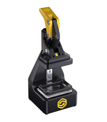
BAL
This BAL design was specially developed for small circuit boards.
Double-sided contacting is also possible with this.
BAL
PRL
POL
IDL
INDIVIDUAL



PRL
The PRL design is particularly suitable for small and medium-sized boards.
It is characterized by very good usability and good accessibility of the circuit board when clamped.
PRL

BAL
POL
IDL
INDIVIDUAL


POL
The POL design is suitable for large boards. It can hold down the circuit board at any point and make double-sided contact if necessary.
The robust mechanism allows contacting hundreds of test points.
POL
BAL
PRL
IDL
INDIVIDUAL

IDL
The IDL test fixture combines a sturdy aluminium frame with linear contacting.
It can be configured for different assembly sizes, high contact counts and contacting from below, above and the side.
IDL
INDIVIDUAL
POL
PRL
BAL


INDIVIDUAL
Are our standardized needle adapters not suitable?
We manufacture custom solutions for you, e.g., for assemblies in housings or contacts on different sides
Individual adapters
BAL

PRL
POL
IDL


Individual Features
Additive manufacturing gives us the freedom to tailor each PCB test fixture to unusual DUT geometries, dense contact layouts and integrated functions. This is especially valuable for compact bed-of-nails test fixtures where mechanics, contacting and interfaces must fit into a small space.

Display and controls in the test fixture

Side contact

Sensors in the test fixture

Exemption of certain areas of the test item

Test needles from any manufacturer or we will make a suggestion

Electronic components permanently installed in the PCB test fixture (e.g. ISP, measurement cards, multiplexers, etc.)

Contacting of test points, pads, vias, solder joints, connectors, …
Ordering Process
Step 1
Calculate price
Simply calculate the expected cost of your PCB test fixture yourself using our price calculator .
We ask for your understanding that the costs may vary depending on individual requirements.
Step 2
Inquiries
Send us your requirements for the PCB test fixture. In particular, we need:
- Number of test points
- Dimensions and shape of the board
- Information about large, heavy or protruding components
- Plugs to be released
- Are currents over 1 ampere flowing?
- Special requirements
Possible data formats:
Photos / Screenshots / Drawings
3D data of the test object (.stp / .iges)
2D data of the test object (.dxf)
Please use our contact form
Step 3
Inquiries / Offer
We always endeavour to process your queries within 24 hours in order to be able to provide you with an individual offer for your PCB test fixture as quickly as possible. If you have any queries, you can reach us at the email address info@eloprint.de, the telephone number +49 711 50480481 or via the following contact form.
Step 4
Order
When ordering, we ask you to provide a test sample for testing purposes. This will of course be returned to you undamaged together with the PCB test fixture.
Step 5
Development / Manufacturing
As soon as we receive your order, we start designing your test fixture. Once we receive your test piece, we can check the tolerances and smooth functioning and then production can be completed.
Step 6
Delivery
We will hand over your test fixture to a suitable shipping service provider within the agreed delivery time.
Press reports about test fixtures from ELOPRINT





Frequently asked questions
Contact
Please enter your contact details in the contact form on the right and describe your requirements for your PCB test fixture. We will get back to you shortly.
To ensure a smooth process, we ask you to fill out the template linked below and upload it. This allows you to specify the coordinates of your test points. You can also specify the desired pin assignment for the adapter interface and any special features such as high currents or RF signals. You are also welcome to add any other requirements for your PCB test fixture to this document.
Contact us at:
+49 711 50480481
Please fill out the contact form for initial contact: